Coma News
Community
News
HOME > News
AI Chips Shifting from Round to Rectangular
As the demand for AI and high-performance computing (HPC) accelerates, the semiconductor packaging industry is undergoing a major transformation — moving from round silicon wafers to rectangular panels.
This shift is being driven by advanced-packaging requirements that push the limits of integration and yield. Toolmakers like Lam Research and Nikon are now offering panel-level production equipment, with Lam forecasting industry-scale adoption by 2027.
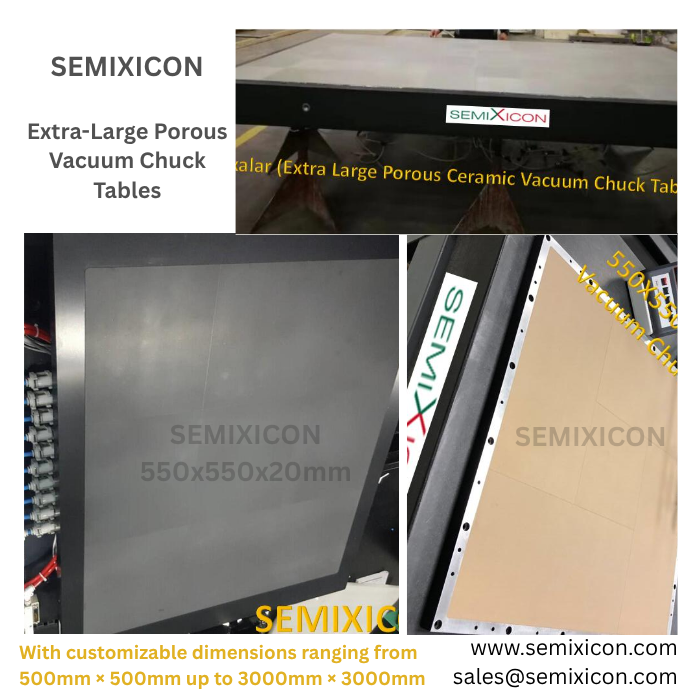
Cerameric Semixicon is catching this trend of transition closely and starting to supply extra large porous ceramic chuck tables with sizes of 310x310; 510x515;600x600;1064x991;1064(701x701) mm etc
Meanwhile, TSMC, long the leader in heterogeneous integration for AI chips from NVIDIA and AMD, may see competition intensify as OSATs (Outsourced Semiconductor Assembly and Test companies) ramp up capabilities to claim a larger share of this fast-growing segment.
According to Yole Group (March 2024), the Panel-Level Packaging (PLP) market — currently valued at $160 million — is projected to quadruple to $650 million by 2030, powered by the rise of AI and HPC.
Key players include:
Samsung Electronics and ASE Global, long-time leaders in advanced packaging
Amkor Technology, Rapidus Corporation, and even TSMC, all developing next-gen fan-out PLP technologies
The rectangular era of chip packaging is coming — faster, denser, and smarter.
#wafer chips #Panel level packaging# Extra large porous ceramic chuck#Vacuum Chuck#Cerameric # SEMIXICON
310x310; 510x515;600x600;1064x991;1064(701x701)

 Preview
 Next
Next