

Coma News
Community
News
HOME > News
TaC Coatings for Semiconductor Manufacturing
As wide-bandgap semiconductors continue to advance toward larger wafer diameters, higher crystal quality, and longer production cycles, materials used in high-temperature process environments are facing unprecedented demands. Among the emerging protective coating technologies, chemical vapor deposited (CVD) tantalum carbide (TaC) coatings have become one of the most promising solutions for next-generation crystal growth and epitaxial processing equipment.
What is a TaC Coating?
Tantalum carbide (TaC) is an ultra-high-temperature ceramic (UHTC) with exceptional thermal and chemical stability. It exhibits a melting point approaching 3,880°C, a density of approximately 13.9 g/cm³, thermal conductivity of around 22 W/m·K, and a coefficient of thermal expansion (CTE) of approximately 6.3 × 10⁻⁶/K. More importantly, TaC demonstrates outstanding chemical inertness against aggressive semiconductor process environments containing silicon vapor, hydrogen, ammonia, and other reactive species.
A TaC coating is typically deposited onto high-purity graphite, carbon-carbon (C/C) composites, porous graphite, or silicon carbide ceramics using chemical vapor deposition (CVD). Industrial deposition commonly employs precursor systems such as TaCl₅–hydrocarbon–H₂–Ar, producing dense, high-purity coatings with excellent adhesion and precisely controlled thickness.
Compared with conventional protective coatings, CVD TaC offers superior density, purity, dimensional control, and long-term stability, making it particularly attractive for contamination-sensitive semiconductor applications.
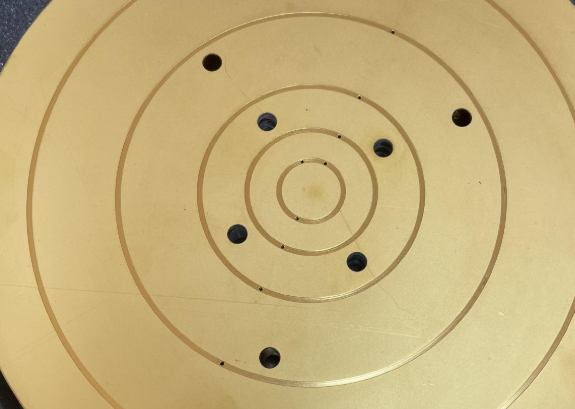
Why the Semiconductor Industry is Transitioning to TaC Coatings
The rapid commercialization of SiC and GaN power devices has significantly increased requirements for crystal growth equipment operating under extreme temperatures and corrosive process atmospheres.
During Physical Vapor Transport (PVT) growth of SiC single crystals, furnace temperatures typically range from 2,000–2,500°C under low-pressure conditions. High-purity graphite components—including crucibles, guide tubes, seed holders, and thermal insulation structures—are continuously exposed to silicon vapor at elevated temperatures.
Although SiC-coated graphite has been the industry standard for many years, prolonged exposure above approximately 2,200°C can lead to coating degradation, silicon attack, graphite erosion, and particle generation. Carbon particles released from deteriorating graphite may become incorporated into growing crystals, leading to defects such as carbon inclusions, polycrystalline nucleation, micropipes, and reduced crystal yield.
As crystal diameters continue expanding from 6-inch to 8-inch and beyond, process cycles become longer and thermal environments more demanding. Conventional SiC coatings increasingly approach their performance limits, driving industry adoption of more robust TaC protective coatings.
Key Applications of TaC Coatings in Semiconductor Manufacturing
1. SiC PVT Crystal Growth Thermal Field Components
The largest and fastest-growing application of TaC coatings is within SiC crystal growth furnaces.
Critical components—including crucibles, seed holders, guide rings, flow tubes, furnace lids, and porous graphite structures—are increasingly protected with CVD TaC coatings.
These coatings provide multiple benefits:
Prevent silicon vapor from reacting with graphite substrates
Suppress graphite erosion and particle generation
Reduce carbon contamination within the growth chamber
Improve thermal field stability and gas flow uniformity
Minimize edge polycrystal formation
Extend component service life through multiple growth cycles
Enhance crystal quality and process repeatability
Porous TaC-coated graphite structures can also function as particle filters while simultaneously improving gas distribution during crystal growth.
2. MOCVD and Epitaxial Growth Equipment
TaC coatings are also gaining attention for GaN and SiC epitaxial reactors, particularly within Metal-Organic Chemical Vapor Deposition (MOCVD) systems.
Graphite susceptors, wafer carriers, showerheads, and other reactor components operate continuously under aggressive environments containing:
High-temperature ammonia
Hydrogen-rich reducing atmospheres
Metal-organic precursor gases
Compared with conventional SiC coatings, TaC provides:
Higher chemical stability
Lower corrosion rates
Superior resistance to peeling and particle generation
Improved contamination control
Longer maintenance intervals
For GaN epitaxy operating at approximately 1,050–1,100°C, TaC effectively protects graphite from atomic hydrogen generated by ammonia decomposition.
For SiC epitaxy at 1,550–1,650°C, where traditional SiC coatings approach their thermal limits, TaC offers a promising next-generation coating technology capable of supporting higher process stability and longer equipment lifetime.
3. Advanced High-Temperature Semiconductor Processes
Beyond SiC crystal growth, TaC coatings are expanding into a variety of demanding semiconductor applications, including:
AlN single-crystal growth systems
Ultra-high-temperature ceramic processing
High-temperature annealing equipment
Semiconductor furnace components
Fluidized-bed reactors for granular silicon production
Specialty vacuum processing equipment
In many of these environments, TaC provides superior resistance to aluminum vapor, halogen-containing process gases, and extreme thermal cycling compared with conventional SiC-coated graphite.
 Preview
 Next
Next